Research & Outreach Centers
Electrical Engineering and Computer Science
- Center for Irradiation of Materials (CIM)
Sponsored by: Department of Defense (DOD), Department of Energy (DOE) and NASA
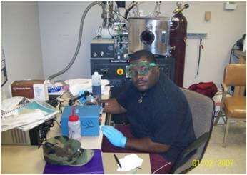
Electrical Engineering students fabricate and characterize high efficient thermoelectric devices for thermoelectric generator and thermoelectric cooling applications. They use the Electrical Engineering Clean Room and Center for Irradiation of Materials (CIM). Our students start learning the basics by working in the laboratory and increase their level of technical sophistication by working closely with faculty. The importance of thermoelectric devices is due to their utility in production of electricity from wasted heat especially in car engines. CIM instruments include a wide array of fabrication and characterization tools including Ion Beam Assisted Deposition system (IBAD), Molecular Beam Epitaxy (MBE), DC/RF Sputtering, Atomic Force Microscopy (AFM), Raman Spectroscopy, XPS, Optical Absorption Spectroscopy, Photoluminescence Spectroscopy, Seebeck Coefficient measurement system, Electrical Conductivity and thermal conductivity systems, Scanning Electron Microscopy (SEM), High energy beam Accelerators, Rutherford back Scattering Spectroscopy (RBS) etc..
- Reconfigurable Computational Laboratory
Sponsored by: Missle Defense Agency (MDA)
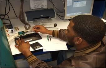
The Reconfigurable Computational Laboratory is dedicated to development of embedded hardware devices for computational algorithms. Primary hardware targets are FPGA, and Microprocessor platforms. The lab contains a number of FPGA development boards from Digilent, Inc. The primary device utilized by students is the NEXYS 2 board with a Spartan 2 FPGA (Xilinx) and a 16 megabyte static ram chip. This board has many general purpose interface devices and connections and is suitable for project development. It uses a general USB cable interface to LINUX or Windows PC’s, and the Xilinx software development environment works with either operating system. The BEE3, a large multi-FPGA system from BEECube, Inc. is hosted in the lab as well.
VHDL language is the primary means for specification of digital circuitry, but can become cumbersome for large-scale project. Impulse C (IMC) from Impulse Technologies is also being used to develop prototype FPGA algorithms within the lab. This structured language process design is based on an input/output data stream approach. The user defines the input and output data streams and specifies how the intermediate processes interconnect. Once this data flow is determined the user specifies the processes logic functions. Examples of serial processes using multiple inputs have been tested. The input streams are unlike traditional programming input/output streams in that the FPGA chip allows for asynchronous, synchronous, and vastly parallel data movement and logic processes. Thus the “high level” nature of Impulse C still requires the careful logic and data movement design processes. The advantage is that once a parallel process has been defined in the structured manner of IMC the actual implementation is left to the resource allocation phase which attempt to use all available FPGA resources. The user does not have to manually do this difficult task.
Back to Top - Microelectronic Characterization Laboratory
Sponsored by: Air Force Office of Scientific Research (AFOSR) and Missile Defense Agency (MDA)
The experimental facilities in the characterization laboratory include impedance spectroscopy, C-V analysis, and Scanning Electron Microscopy with Energy Dispersive Spectroscopy (SEM-EDS). A wide range of semiconducting materials and devices are characterized in this laboratory. The impedance spectroscopy is accomplished via HP4192A LF Impedance Analyzer covering frequency range 5 Hz through 13 MHz. The HP4145 C-V Analyzer is capable of providing Mott-Schottky data for nonlinear devices. The state-of-the-art JEOL 6610 SEM and Oxford EDS system is used for analyzing materials and devices including elemental analysis. The characterization laboratory is extensively used by students to accomplish their Senior Design projects.
Back to Top - Selected Publications
Below are selected publications by EECS Students and Faculty related to Center for Irradiation of Materials (CIM) Activities:
- S. Budak, J. Chacha, C. Smith, M. Pugh, K. Heidary, R. B. Johnson , D. ILA, “Effects of MeV Si ion bombardment on the thermoelectric generator from SiO2/SiO2 + Cu and SiO2/SiO2 +Au nanolayered multilayer films”, Nuc. Instr. and Meth. B , 2011 (in press).
- J. Chacha, S. Budak, C. Smith, D. McElhaney, M. Pugh, K. Ogbara, K. Heidary, R. B. Johnson, C. Muntele, D. ILA, “Thermoelectric Properties of SiO2/SiO2+Au Nano-layered Superlattices Modified by MeV Si ions beam”, AIP Conf. Proc. 1336, 257-259 (2011) for CAARI 2010 21st International Conference on the Application of Accelerators in Research and Industry, August 8 – 13, 2010, Fort Worth, Texas USA.
- C. Smith, S. Budak, J. Chacha, M. Pugh, B. Chhay, K. Heidary, R. B. Johnson, C. Muntele, D. Ila, “Photoluminescence and X-ray photoelectric Spectroscopy of MeV Si Ion Bombarded SiO2/SiO2+Cu Multilayer films” Mater. Res. Soc. Symp. Proc. Vol.1354 (2011), (in press).
- S. Budak, C. Smith, J. Chacha, M. Pugh, K. Ogbara, K. Heidary, R. B. Johnson, C. Muntele, D. ILA, “Thermoelectric Generator from SiO2/SiO2+CoSb multi-layer Nanolayered Films Modified by MeV Si Ions Bombardment Mater. Res. Soc. Symp. Proc. Vol. 1267 © 2010 Materials Research Society 1267-DD05-13.
- J. Chacha, S. Budak, C. Smith, M. Pugh, K. Ogbara, K. Heidary, R. B. Johnson, C. Muntele, D. ILA, “Thermoelectric Generator from SiO2/SiO2+Cu Nanolayered Multilayer films Effected by MeV Si Ions Bombardment”, Mater. Res. Soc. Symp. Proc. Vol. 1267 © 2010 Materials Research Society 1267-DD05-15.
- M. Pugh, S. Budak, C. Smith , J. Chacha, K. Ogbara, K. Heidary, R. B. Johnson , C. Muntele, D. ILA, “Fabrication and Characterization of Thermoelectric Generator from Si/Si+Ge multi-layer superlattice Nanolayered Films Effected by MeV Si Ions Bombardment”, Mater. Res. Soc. Symp. Proc. Vol. 1267 © 2010 Materials Research Society 1267-DD05-14.
- C. Smith, S. Budak, J. Chacha, M. Pugh, H. Martin, T. Langham, B. Harrell, K. Heidary, R. B. Johnson, Y. Yang, C. Muntele, D. ILA, “Thermoelectric Properties of Thermoelectric Generator From SiO2/SiO2+Ag Nanolayered Multilayer Films Effected by MeV Si Ions”, Mater. Res. Soc. Symp. Proc. Vol. 1267 © 2010 Materials Research Society 1267-DD05-16.
- C. Smith, M. Pugh, H. Martin, R. Hill, B. James, S. Budak, K. Heidary, C. Muntele, D. ILA, “ Thermoelectric Generators of Sequentially Deposited Si/Si+Ge Nano-layered Superlattices”, Mater. Res. Soc. Symp. Proc. Vol. 1181 © 2009 Materials Research Society, 1181-DD02-04
- M. Pugh, R. Hill, H. Martin, B. James, C. Smith, S. Budak, K. Heidary, C. Muntele, D. ILA, “Fabrication and Characterization of Thermoelectric Generators From SiO2/SiO2+Au Nano-layered Superlattices”, Mater. Res. Soc. Symp. Proc. Vol. 1181 © 2009 Materials Research Society, 1181-DD13-05
- S. Budak, S. Guner, T. Hill, M. Black, S. B. Judah, C. Muntele, and D. Ila, “Fabrication and Characterization of Thermoelectric Generators From SiGe Thin Films”, Mater. Res. Soc. Symp. Proc. Vol. 1102E © 2008 Materials Research Society 1102-LL05-03.